While preparing an ATV demonstration for a local club recently, I realised that one of my converted ex-satellite receivers would not display its on-screen menu unless it had sync pulses to lock to. I only had one of my test card generators to hand so an alternative portable sync source had to be found quickly. The simple designs featured in early copies of CQ-TV either were impractical to build quickly or didn't produce the interlaced scans I needed. For some time I had been bouncing the idea in my mind of using a very simple microcontroller to produce sync patterns in software rather than the usual method of using counter chips and logic gates. After much head scratching and some challenging software writing, the design shown here was born.
The syncs are for 625 line 50Hz television, unfortunately it isn't possible to produce 525/60Hz scans with sufficient accuracy from such a simple circuit because the smallest time interval that can be produced in software is inadequate for the fractional microsecond timings that NTSC needs. In fact some liberties have been taken with the PAL timings but they are better than 99.9% correct and should be good enough fool almost all video equipment. An NTSC version can be produced but the cost is significantly higher because a quartz crystal and slightly more complicated microprocessor would have to be used. All the parts in the PAL design can be purchased for less than 50 pence, that's about 70 US cents!
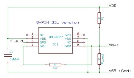
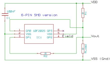
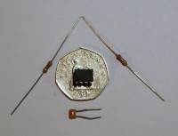
The prototype used an 8-pin DIL chip and wire ended resistors but an SMD version of the chip with 6 pins (two are unused in the 8-pin package) and SMD resistors will work equally well. If SMD parts are used, the whole SPG will fit inside a normal BNC plug!
The chip can be either a PIC10F202 or a PIC10F206, the only difference between these devices is that the '206 has an internal voltage comparator which is not present in the '202 version. The comparator is not used in this design and instructions are present in the code to disable it. The disabling instructions are ignored in the '202 so the same code work in both devices.
How it works:
Buried inside the PIC is a 4MHz oscillator, it isn't crystal controlled but it is very stable and tunable to make it very accurate. The output from the oscillator is divided by four to produce an instruction clock. One instruction, with the exception of jump and some compare instructions, is executed per instruction clock. The frequency instructions are executed is therefore 4Mhz/4 or 1MHz and each instruction takes 1/1MHz of a second to execute, in more meaningful units this is 1 microsecond.
If you imagine an instruction to drive a pin high followed by an instruction to drive it low, you would take two 1MHz cycles, going hight for 1uS then low for 1uS and produce an output signal at 500KHz.
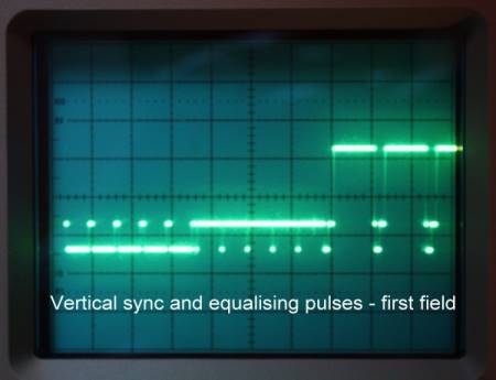
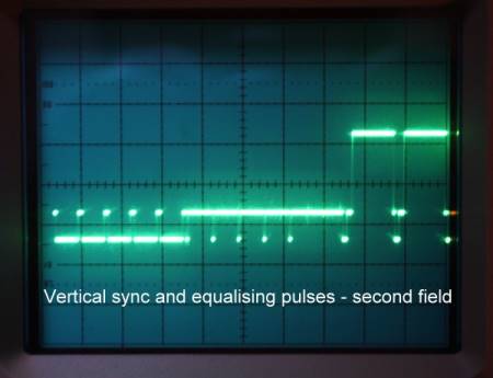
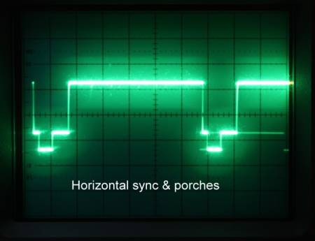
To make video sync signals, a string of instructions has to be used to drive a pin high or low at the correct time intervals. In a 625 line system, each horizontal sync pulse is 4.7uS long and the rest of the line takes 59.3uS making a total of 64uS. Because of the instruction clock speed, the best that can be achieved in this design is 1uS resolution so the timings are approximated as 5uS and 59uS. So each line starts with the output pin being driven low for 5 instructions then driven high for 59 instructions. While this sounds easy, it would take exactly 40,000 instructions to complete one picture scan but the chip only has 512 memory addresses to hold them! Several program loops in which the same instructions are repeated several times are used to keep the memory requirements down to a practical size. In fact by using delay loops the memory requirement is reduced from 40,000 bytes to just 285 bytes. By far the most complicated timing to get right was the vertical sync pulses. Although simple SPGs usually use single broad pulses, I decided in this design to follow the specifications as closely as possible. Vertical sync pulses are actually a complicated sequence of different pulse widths and are different on alternate scans. They alternate so that there is a short delay on every second scan so that lines are aligned slightly differently to produce interlacing. This design does produce interlaced syncs and one of the pins is used to indicate which of the two fields is currently being produced. The pin is low (0V) for lines 1 to 312.5 then high (VDD) until the end of line 625. I can't think of a practical use for this at the moment but it costs nothing and it uses a spare pin so I included it in the coding.
The 50p Sync Pulse Generator.
This article appears in CQ-TV magazine, issue 226.
The field output on GP2 is actually the only signal that is driven high and low, the other two outputs are permanently driven low but they are changed from being inputs to outputs to simulate a switch to ground. When the pin is set to be an input it draws negligible current and the external resistors wired to it will decide the voltage present on it. When switched to output mode, being driven low, they sink current to ground and pull the voltage close to zero. In essence a very simple two-bit digital to analogue converter is implemented with the output voltages representing sync tip (0V), black level (0.3V) and a single video level which you select yourself from 0.3V to 1V (black to peak white).
The two resistors, in conjunction with the load will, depending on which output pins are sinking current, set the video and black level voltages. GP0 is the pin carrying sync information and GP1 carries a signal very similar to the visible part of scan lines. When both are outputs, they pull the voltage across the load down to almost zero, this sets the bottom of the sync pulses. When GP0 and GP1 are inputs, the voltage is set solely by the potential divider formed by R1 and the load resistance. This is your selected white level. If a resistor (R2) is fitted between GP1 and the load, and GP1 is sinking current, it will pull the output voltage lower than peak white level so any 'brightness' between black and white can be set. Lower values of R2 will increase the sink current and reduce the video voltage. The actual values of R1 and R2 depend on the supply voltage and the load resistance. The chip will run quite happily from a supply of 2V up to 5.5V although at the lower end of the range you will find the resistor values become quite low and there is a risk of exceeding the current rating of the pins on the chip during sync periods. The chip manufacturer quotes the absolute maximum current allowed is 75mA which equates at 2V supply to R1 being just 27 Ohms when the load is 75 Ohms. If the supply voltage is kept at or above 3V there is no risk of exceeding the ratings. Trying to produce a standard 1V video signal from a supply of just 2V isn't a likely scenario anyway.
To keep costs down the bottom resistor in the potential divider is the load resistor which should be present across the input of the device being driven, typically this would be 75 Ohms. Slightly better linearity can be achieved by adding a buffer amplifier after the potential divider. When higher load impedances are fed, the values of R1 and R2 can be made much larger which improves linearity and reduces the overall current consumption. The downside to this is the extra expense which would break the 50p budget. It may still be possible to build the SPG and a discrete transistor buffer for under £1 but I leave that to your ingenuity. Unfortunately, the outputs of the chip have a small but measurable resistance so there will always be a residual voltage on them when sinking current to ground. This voltage is proportional to the current in R1 and the load so minimising it is another good reason to use larger values and a buffer stage.
The tables show suggested resistor values when using 5V or 3.3V supplies and standard resistor values for the load. Very few values for R1 and R2 are available off the shelf but using the nearest standard value will still give a very good approximation to the desired levels. As mentioned earlier, the internal resistance of the chip drivers also have some influence on the output voltage but for practical purposes they can be ignored. For a normal 5V supply and 75 Ohm load, using 300 Ohms for R1 and 27 Ohms for R2 will give good results.
Note: The tables are rather large to place on a web page so you can either look at them in CQ-TV magazine (www.cq-tv.com) or use the spreadsheet in the downloads section to calculate them yourself. There are two files, RValues.xls and Rvalues.ods, which have identical contents. The xls version is for MS Excel and the odt version is for OpenOffice Calc. All you have to do is enter the supply voltage and required video level in the blue boxes and the table of R1 and R2 values will be generated automatically for a selection of standard load resistances. You can adjust the load manually by typing other numbers in the load column, R1 and R2 will be calculated accordingly. The detached column is Rparallel which is used in the calculation but is not a physical component.
For the purist, this is how the values of R1 and R2 are calculated:
1.Pick Rload according to your requirements.
2.Calculate R1 with the formula: R1=((VDD-Vout)*Rload)/Vout.
3. Work out the value of R1 and R2 in parallel needed to set black level (Vout =0.3V)
with the formula: Rparallel = (Vout * R1)/(VDD-Vout).
4.Extract the value for R2 with the formula: R2=1/((1/Rparallel)-(1/Rload))
Rparallel isn't a real component, it is only used to simplify the calculation.
Programming the PIC.
I use a device called PICkit 2 from the chip manufacturer. It cost £9.99 including postage and VAT as part of a special offer in a magazine recently. Microchip have recently introduced a new model called PICkit 3 so the older devices are being discounted to empty the shelves. If you really want to make a programmer on the cheap, the complete design for PICkit is on the Microchip web site at www.microchip.com and it includes all the software inside the PICkit and the program to drive it from a PC. It connects through a USB cable and programs hundreds of different microcontrollers and memory devices, in most cases drawing power from the computers USB port itself. The SPG program was written in assembly language using MPLAB which is also free of charge on Microchips web site.
I would caution you over the chip calibration. The internal clock is trimmed by the manufacturer to be 4MHz with better than 1% accuracy. To calibrate it, a number has to be loaded into the OSCCAL register inside the chip. Normally, this would be done by the first instruction in a program and that is exactly what is done in this SPG. While testing the chip the manufacturer determines the best value and leaves it in the chips memory so it can be picked up and moved into OSCCAL. That is where you can run into problems if you are not aware of the calibration value. If you inadvertently erase the chips memory, you lose the calibration value as well. The PICkit automatically reads the value before erasing or re-programming the chip and puts it back afterwards but some other programmers may not do this. What I do is read all the chips as I get them and write the value on the underside of the chip just in case it gets erased. If all else fails, PICkit has a facility to write a test program into the chip, analyse its output and recalculate the calibration value for you. I'm not sure how far off frequency a chip could be if isn't calibrated but my guess is it would be pretty close to correct no matter what value you used. The value is an eight-bit number in which the least significant bit is always a zero. Setting all bits to zero puts it in the centre of its adjustment range.
The code for the PIC is "50p_spg.hex" which is available by clicking here.
The PIC devices are available from Farnell, Crownhill Associates, Microchip Direct and many other sources at prices around 35p +VAT.
While not perfect, this should make a useful addition to your video toolkit and I don't think you can grumble at the price!